| CPC C03C 19/00 (2013.01) [C03C 17/3417 (2013.01); C03C 2217/734 (2013.01); C03C 2218/154 (2013.01); G02F 1/133302 (2021.01); G02F 1/133331 (2021.01); G06F 1/1652 (2013.01); Y10T 428/24355 (2015.01)] | 21 Claims |
|
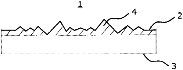
1. A glass sheet comprising a first main surface and a second main surface opposing the first main surface, wherein
the glass sheet has an affected layer directly below the first main surface,
in at least a part of the first main surface, an average element length RSm is from 2,500 nm to 6,000 nm, a root-mean-square height Sq is from 3 nm to 45 nm, and a skewness Ssk is a negative value,
an absolute value of a warpage of the glass sheet is 200 μm or less, and
the affected layer has a total thickness of from 30 nm to 500 nm.
|
|
13. A glass sheet comprising a first main surface and a second main surface opposing the first main surface, wherein
the glass sheet has an affected layer directly below the first main surface,
in at least a part of the first main surface, an average element length RSm is from 2,500 nm to 6,000 nm, a root-mean-square height Sq is from 3 nm to 45 nm, and a skewness Ssk is a negative value,
an absolute value of a difference between an Al/Si value in the first main surface and an Al/Si value in the second main surface is 0.1 or less, provided that Al is a peak area of the Al2p binding energy peak measured by X-ray photoelectron spectroscopy and Si is a peak area of an Si2p binding energy peak measured by X-ray photoelectron spectroscopy, and
the affected layer has a total thickness of from 30 nm to 500 nm.
|