| CPC B81B 3/0024 (2013.01) [B81B 3/0021 (2013.01); B81B 7/02 (2013.01); H04N 23/57 (2023.01); H04N 23/67 (2023.01); B81B 2201/032 (2013.01); B81B 2201/047 (2013.01); B81B 2203/0127 (2013.01); B81B 2203/0172 (2013.01); B81B 2203/0315 (2013.01); B81B 2203/04 (2013.01); B81B 2203/053 (2013.01)] | 20 Claims |
|
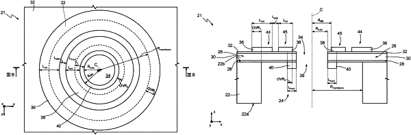
1. A method, comprising:
forming a first etch stop layer on a first surface of a substrate;
forming a first epitaxial layer on the first etch stop layer and on the first surface of the substrate;
forming a second etch stop layer on the first epitaxial layer;
forming a second epitaxial layer on the second etch stop layer;
forming a first piezoelectric actuator and a second piezoelectric actuator on the second epitaxial layer spaced apart from each other; and
forming a cavity extending through the substrate, the first epitaxial layer and the second etch stop layer.
|