| CPC B29C 33/42 (2013.01) [H01L 21/565 (2013.01)] | 10 Claims |
|
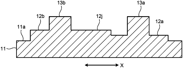
1. A template comprising a transferring pattern on a first surface of a substrate,
the transferring pattern including:
a first projecting portion that projects from the first surface with a first height and extends along the first surface;
a second projecting portion that projects from the first surface with a second height higher than the first height and extends along the first surface;
a first columnar portion that is arranged at a position overlapping with the first projecting portion and has a top surface with a third height higher than the second height, the third height being a height from the first surface; and
a second columnar portion that is arranged at a position overlapping with the second projecting portion and has a top surface with the third height,
wherein a first width of the first projecting portion in a first direction along the first surface and intersecting with an extending direction of the first projecting portion is narrower than a second width of the second projecting portion in a second direction along the first surface and intersecting with an extending direction of the second projecting portion.
|