| CPC A61B 6/145 (2013.01) [A61B 6/4233 (2013.01); G01T 1/247 (2013.01)] | 12 Claims |
|
1. Intraoral radiological image sensor using MOS technology comprising:
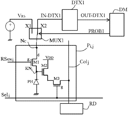
a matrix (M-PIX) of first photosensitive pixels arranged in rows and columns, each pixel (Pij) comprising a photodiode (PH) and a plurality of transistors, the plurality of transistors including a photodiode initialisation transistor (M1) connected between a photodiode node (KNi) of the pixel and a first connection node (NC) common to the first photosensitive pixels;
a sequencing circuit (DM) supplying signals for commanding the plurality of transistors of each of the first photosensitive pixels for controlling an image capture sequence (300) during exposure to an X-ray flash (FX), comprising a phase of overall initialisation (301) of the photodiodes of the first photosensitive pixels, a phase of integrating charges (302) during an integration period and a phase of reading (303) the first photosensitive pixels;
wherein the sensor comprises a first coupling switch (MUX1) controlled by a first logic signal (PROB1) for connecting said first connection node (NC) to a signal input (INDTX1) of a first current detection circuit (DTX1) or to a photodiode initialisation voltage source (VRS), whereby said first logic signal is changeable between a first logic state and a second logic state;
the sequencing circuit (DM) of the sensor being configured to control a phase (200) of detecting, by said first detection circuit (DTX1), the start of exposure to an X-ray flash for triggering the image capture sequence (300), comprising the following operations:
commanding the photodiode initialisation transistors (M1) to switch to the on-state in all the first photosensitive pixels simultaneously; and
establishing the first logic signal (PROB1) in said first logic state, the effect of which is to inject, at the signal input (IN-DTX1) of the first detection circuit, a current (I) collected on said first connection node (NC) originating from the photodiodes of the first photosensitive pixels; then
establishing, when an output logic signal (OUT-DTX1) of the first detection circuit toggles from a first output logic signal state to a second output logic signal state, corresponding to the detection of an input current level above a predetermined threshold, the first logic signal (PROB1) in said second output logic signal state, the effect of which is to couple said initialisation transistors (M1), which are always in the on-state, to said initialisation voltage source (VRS), thus activating the phase of overall initialisation (301) of the image capture sequence, for initialising the photodiodes before said integration phase; and
wherein the first detection circuit (DTX1) comprises a capacitive transimpedance amplifier (CTIA1) comprising a noninverting input connected to a common mode voltage (Vcm1) and an inverting input, which forms the signal input (IN-DTX1), which is coupled to said first connection node (NC), said amplifier being controlled by a clock signal (Φctia) for periodically producing, at a signal output (Vout-ctia1) of said amplifier, a voltage ramp as a function of the level of the current injected at the signal input, which ramp is applied to a comparator (COMP1) for comparison to a voltage threshold value (Vth1).
|