| CPC A61B 5/1486 (2013.01) [A61B 5/1468 (2013.01); A61B 5/1473 (2013.01); A61B 5/14532 (2013.01); A61B 5/14546 (2013.01); A61B 5/4839 (2013.01); A61B 5/6848 (2013.01); H05K 3/325 (2013.01); A61B 2562/164 (2013.01); A61B 2562/227 (2013.01); H01L 24/72 (2013.01); H01L 2924/07811 (2013.01); H01L 2924/12042 (2013.01); H05K 3/365 (2013.01); H05K 2201/053 (2013.01); H05K 2201/10151 (2013.01); H05K 2201/10401 (2013.01); H05K 2201/10409 (2013.01); Y10T 29/4913 (2015.01)] | 17 Claims |
|
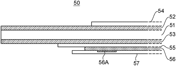
1. An electrode arrangement, comprising:
a base substrate having a width;
a first conductive layer having a width (W1) and positioned on the base substrate;
a second conductive layer having a width (W2), wherein W1 is less than W2, and
a dielectric layer having a width and positioned between the first and second conductive layers.
|