| CPC H10N 70/063 (2023.02) [H10B 63/00 (2023.02); H10N 70/028 (2023.02); H10N 70/041 (2023.02); H10N 70/841 (2023.02); H10N 70/8833 (2023.02)] | 11 Claims |
|
1. A method for forming a semiconductor structure, comprising:
providing a substrate;
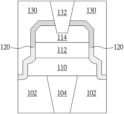
forming a resistance random access memory on the substrate, wherein the resistance random access memory comprises an upper electrode, a lower electrode and a resistance conversion layer between the upper electrode and the lower electrode; and
forming a cap layer on the resistance random access memory, wherein the cap layer has an upper half and a lower half, and the upper half and the lower half contain different stresses.
|