| CPC H10N 50/80 (2023.02) [G11C 11/161 (2013.01); H01F 10/329 (2013.01); H01F 10/3259 (2013.01); H10B 61/22 (2023.02); H10N 50/01 (2023.02); H01F 10/3286 (2013.01); H10N 50/85 (2023.02)] | 20 Claims |
|
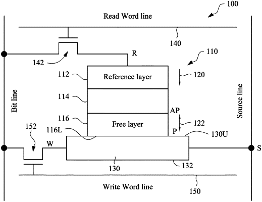
17. A method, comprising:
forming a transistor over a substrate, the transistor having a first source/drain terminal, a second source/drain terminal and a gate terminal;
forming a magnetoresistive random access memory cell over the transistor, the magnetoresistive random access memory cell including a magnetic tunnel junction structure and a spin-orbit torque structure adjacent to the magnetic tunnel junction structure;
forming a write signal line coupled to the gate terminal; and
forming a first current node coupled to the first source/drain terminal;
wherein a first end of the spin-orbit torque structure coupled to the second source/drain terminal, and a second end of the spin-orbit torque structure coupled to a second current node; and
wherein the forming the spin-orbit torque structure includes:
forming a first heavy metal layer, a second heavy metal layer stacked over the first heavy metal layer and a third heavy metal layer stacked over the second heavy metal layer;
diffusing a first plurality of molecules of a dielectric material scattered adjacent to an interface between the first heavy metal layer and the second heavy metal layer; and
diffusing a second plurality of molecules of a dielectric material scattered adjacent to an interface between the second heavy metal layer and the third heavy metal layer.
|