| CPC H10K 77/111 (2023.02) [H01L 25/18 (2013.01); H10K 50/844 (2023.02); G02F 1/133305 (2013.01); G02F 1/133331 (2021.01); G06F 1/1641 (2013.01); G06F 1/1652 (2013.01); G09G 3/3266 (2013.01); G09G 3/3275 (2013.01); G09G 3/3283 (2013.01); G09G 3/3291 (2013.01); G09G 2300/0408 (2013.01); H10K 50/115 (2023.02); H10K 50/84 (2023.02); H10K 50/8426 (2023.02); H10K 59/13 (2023.02); H10K 59/88 (2023.02); H10K 2102/00 (2023.02); H10K 2102/311 (2023.02)] | 2 Claims |
|
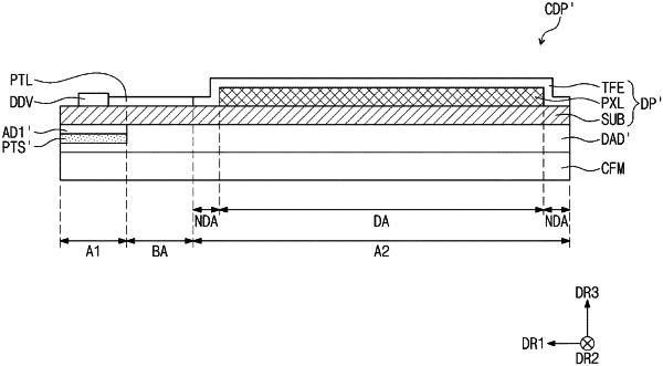
1. A carrier panel comprising:
a substrate including a first region, a second region, and a bending region between the first region and the second region;
a pixel layer disposed on the substrate;
a protective substrate disposed below the substrate;
a first adhesive layer disposed between the substrate and the protective substrate;
a carrier film disposed below the protective substrate; and
a dummy adhesive layer disposed between the protective substrate and the carrier film, wherein
an adhesion of the dummy adhesive layer is weaker than an adhesion of the first adhesive layer, and
the protective substrate has a thickness smaller than a thicknesses of each of the substrate and the carrier film.
|