| CPC H10K 71/00 (2023.02) [H01L 27/124 (2013.01); H01L 27/1222 (2013.01); H01L 27/1255 (2013.01); H10K 59/131 (2023.02); H01L 27/1225 (2013.01)] | 16 Claims |
|
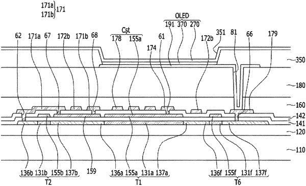
1. An organic light-emitting diode (OLED) display, comprising:
a substrate;
a scan line formed over the substrate and that transfers a scan signal;
a data line and a driving voltage line that respectively transfer a data voltage and a driving voltage and that are thrilled over the substrate;
a switching transistor that includes a switching gate electrode electrically connected to the scan line, a switching source electrode electrically connected to the data line and a switching drain electrode configured to output the data voltage;
a driving transistor that includes a driving gate electrode, a driving drain electrode, and a driving source electrode; and
a connecting member disposed on a same layer as the driving gate electrode,
wherein the driving voltage line includes a first driving voltage line that extends in a first direction and a second driving voltage line that extends in a second direction crossing the first direction, wherein the first driving voltage line in the first direction and the second driving voltage line in the second direction are formed as a whole,
wherein the data line includes a first data line and a second data line separated from the first data line,
wherein the connecting member electrically connects the first data line to the second data line,
wherein a bottom surface of the first driving voltage line and a bottom surface of the second driving voltage line directly contact a same layer,
wherein the first data line and the second data line are disposed at a same layer as the second driving voltage line, and the connecting member crosses and overlaps the second driving voltage line, and
wherein the bottom surface of the connecting member directly contacts a same layer as a bottom surface of the switching gate electrode and the driving gate electrode.
|