| CPC H10K 59/88 (2023.02) [H10K 50/844 (2023.02); H10K 59/124 (2023.02); H10K 59/131 (2023.02); H10K 71/221 (2023.02); H10K 50/11 (2023.02); H10K 59/1201 (2023.02)] | 10 Claims |
|
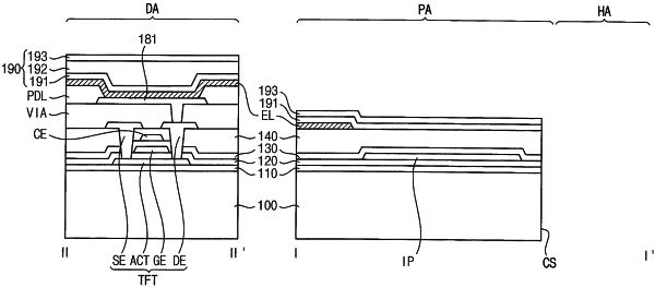
1. A display apparatus, comprising:
a base substrate including a display area, an opening area, and an opening peripheral area between the opening area and the display area, wherein the display area surrounds the opening area, and the opening peripheral area has an annular shape;
a conductive pattern disposed on the base substrate in the opening peripheral area and having an annular shape; and
a light emitting layer disposed on the base substrate and in a portion of the opening peripheral area, and including an organic material, and
wherein the light emitting layer is not formed at a portion of opening peripheral area that is adjacent to the opening area.
|