US 11,793,056 B2
OLED device structure and manufacturing method thereof
Jiajia Sun, Wuhan (CN)
Assigned to WUHAN CHINA STAR OPTOELECTRONICS SEMICONDUCTOR DISPLAY TECHNOLOGY CO., LTD., Hubei (CN)
Appl. No. 16/958,764
Filed by WUHAN CHINA STAR OPTOELECTRONICS SEMICONDUCTOR DISPLAY TECHNOLOGY CO., LTD., Hubei (CN)
PCT Filed Apr. 22, 2020, PCT No. PCT/CN2020/086019
§ 371(c)(1), (2) Date Jun. 29, 2020,
PCT Pub. No. WO2021/139038, PCT Pub. Date Jul. 15, 2021.
Claims priority of application No. 202010008368.8 (CN), filed on Jan. 6, 2020.
Prior Publication US 2023/0157140 A1, May 18, 2023
Int. Cl. H10K 59/80 (2023.01); H10K 77/10 (2023.01); H10K 71/00 (2023.01); H10K 102/00 (2023.01); H10K 59/40 (2023.01)
CPC H10K 59/8794 (2023.02) [H10K 71/00 (2023.02); H10K 77/111 (2023.02); H10K 59/40 (2023.02); H10K 2102/311 (2023.02)] 10 Claims
OG exemplary drawing
 
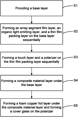
1. An organic light emitting diode (OLED) device structure, comprising:
a base layer, an array segment film layer, an organic light emitting layer, and a thin film packing layer disposed sequentially from bottom to top;
a touch layer, a polarizer, and a cover glass sequentially disposed above the thin film packing layer;
a composite material layer disposed under the base layer; and
a foam copper foil layer disposed under the composite material layer.