| CPC H10K 59/50 (2023.02) [G02F 1/0126 (2013.01); H10K 59/126 (2023.02)] | 15 Claims |
|
1. A display device, comprising:
a substrate where a plurality of sub pixel areas is defined;
a thin film transistor disposed on the substrate;
an organic light emitting diode disposed in each of the plurality of sub pixel areas, comprising:
a first electrode disposed on the thin film transistor;
an organic light emitting layer disposed on the first electrode; and
a second electrode disposed on the organic light emitting layer;
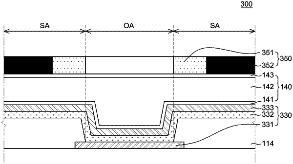
a bank disposed on the thin film transistor to expose at least a portion of the first electrode and separating adjacent sub pixels; and
a black matrix layer disposed on the second electrode and includes a shielding area and an opening area,
wherein the opening area overlaps with an emission area where light is emitted from the organic light emitting layer, and the shielding area overlaps with the bank,
wherein the shielding area includes a variable light shielding unit which varies light transmittance in accordance with incident light and a light shielding unit with a constant light transmittance,
wherein the variable light shielding unit is disposed to enclose the opening area of each of the plurality of sub pixel, and
wherein a width of the variable light shielding unit is 0.3 times to 0.7 times a distance between the organic light emitting layer and the black matrix layer.
|