| CPC H10K 59/40 (2023.02) [G06F 3/0412 (2013.01); G06F 3/0446 (2019.05); G06F 3/0448 (2019.05); H10K 50/84 (2023.02)] | 20 Claims |
|
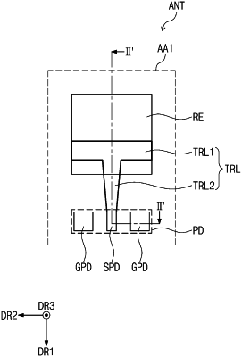
1. A display device, comprising:
a display panel;
a sensing electrode disposed on the display panel;
a transmission line disposed on the display panel and spaced apart from the sensing electrode;
an insulating layer disposed on both the sensing electrode and the transmission line; and
a radiation electrode disposed on the insulating layer,
wherein a portion of the transmission line overlaps a portion of the radiation electrode, and
wherein the insulating layer electrically separates the transmission line from the radiation electrode such that the transmission line does not directly contact the radiation electrode.
|