| CPC H10K 59/40 (2023.02) [H10K 50/15 (2023.02); H10K 50/16 (2023.02); H10K 50/171 (2023.02); H10K 50/865 (2023.02); H10K 50/868 (2023.02); H10K 59/1213 (2023.02); H10K 59/1216 (2023.02); H10K 2102/00 (2023.02)] | 9 Claims |
|
1. A display apparatus comprising:
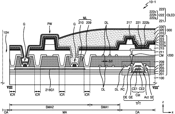
a substrate including a first area, a second area surrounding the first area, and a third area between the first area and the second area, wherein the first area comprises a through hole that extends through the substrate from a first surface to a second surface;
a display layer on the substrate, the display layer comprising:
a display element in the second area of the substrate, the display element comprising a pixel electrode, an opposite electrode, and an intermediate layer between the pixel electrode and the opposite electrode; and
a pixel circuit electrically connected to the display element;
an encapsulation layer on the display layer, a portion of the encapsulation layer being in the third area;
a plurality of touch electrodes on the encapsulation layer, the plurality of touch electrodes being in the second area;
at least one groove in the third area; and
a metal layer on the encapsulation layer, wherein the metal layer overlaps the at least one groove in the third area.
|