| CPC H10K 59/38 (2023.02) [H10K 50/865 (2023.02); H10K 59/40 (2023.02); H10K 71/00 (2023.02)] | 16 Claims |
|
1. A display apparatus, comprising:
a base;
a display layer disposed on a side of the base, the display layer including a plurality of sub-pixels;
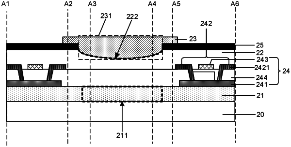
a color filter layer disposed on a display side of the display layer, the color filter layer including a plurality of color resistance portions in one-to-one correspondence with the plurality of sub-pixels, wherein a thickness of any color resistance portion of the plurality of color resistance portions is decreased in a direction away from a reference line of the color resistance portion, and the reference line is a straight line passing through a geometric center of the color resistance portion and perpendicular to the base;
a first insulating layer, wherein a surface of the first insulating layer adjacent to the color filter layer is provided with a plurality of first grooves in one-to-one correspondence with the plurality of color resistance portions; and a depth of any first groove is decreased in a direction away from a reference line of a corresponding color resistance portion; and an orthographic projection of each color resistance portion on the display layer is located within a range of an orthographic projection of a corresponding first groove on the display layer; and a surface of each first groove adjacent to the color filter layer is in contact with a surface of a corresponding color resistance portion adjacent to the first insulating layer;
a touch structure layer disposed on a side of the first insulating layer away from the color filter layer; and
a black matrix provided with a plurality of openings, and the plurality of color resistance portions are in one-to-one correspondence with the plurality of openings;
wherein the touch structure layer includes a plurality of electrodes and a second insulating layer; orthographic projections of the plurality of electrodes of the touch structure layer on the display layer are located within a range of an orthographic projection of the black matrix on the display layer;
the plurality of electrodes include first touch electrodes, second touch electrodes, and bridges, the first touch electrodes and the second touch electrodes are insulated from each other and arranged crosswise; each first touch electrode includes a plurality of first touch sub-electrodes separated by the second touch electrodes, and two adjacent first touch sub-electrodes in the first touch electrode are electrically connected through a bridge; and the bridges and the second touch electrodes are separated by the second insulating layer;
a surface of the second insulating layer adjacent to the first insulating layer is provided with a plurality of second grooves; and the plurality of second grooves and the plurality of first grooves are in one-to-one correspondence, and an orthographic projection of each first groove on the display layer is located within a range of an orthographic projection of a corresponding second groove on the display layer, and a surface of each second groove adjacent to the first insulating layer is in direct contact with a surface of the first insulating layer adjacent to the second insulating layer;
the touch structure layer and the first insulating layer form a first combined structure, and the touch structure layer, the first insulating layer and the color filter layer form a second combined structure;
a difference of a maximum thickness of a portion of the first combined structure whose orthographic projection on the base is located between the orthographic projections of the sub-pixels on the base, and a minimum thickness of a portion of the first combined structure whose orthographic projection on the base overlaps with an orthographic projection of a sub-pixel on the base is ΔH2;
a difference of a maximum thickness of a portion of the second combined structure whose orthographic projection on the base is located between the orthographic projections of the sub-pixels on the base, and a minimum thickness of a portion of the second combined structure whose orthographic projection on the base overlaps with an orthographic projection of a sub-pixel on the base is ΔH3;
ΔH3 is less than ΔH2.
|