| CPC H10K 59/18 (2023.02) [H10K 71/00 (2023.02); H10K 71/851 (2023.02)] | 20 Claims |
|
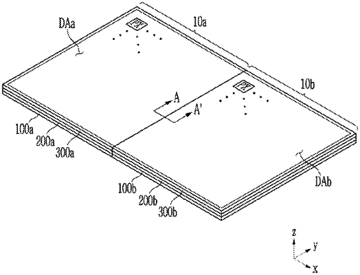
1. A display device comprising:
a substrate;
a first insulating layer disposed on the substrate;
a wire disposed on the first insulating layer; and
a second insulating layer disposed on the wire,
wherein the first insulating layer, the wire, and the second insulating layer extend from an edge of the substrate to overlap a side surface of the substrate.
|