| CPC H10K 59/131 (2023.02) [H10K 59/124 (2023.02); H10K 59/1213 (2023.02); H10K 59/1216 (2023.02); H10K 59/65 (2023.02)] | 15 Claims |
|
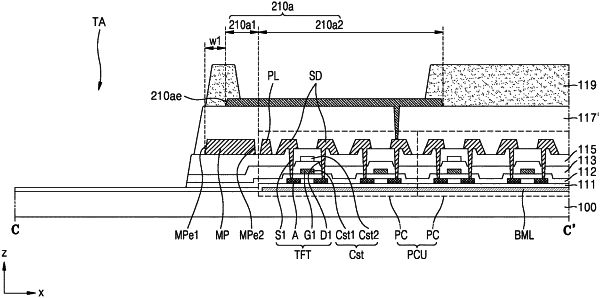
1. A display apparatus comprising:
a substrate including a first area in which a transmissive portion is located and a second area adjacent to the first area;
a pixel circuit unit arranged in the first area and including a pixel circuit;
a first pixel electrode arranged in the first area and electrically connected to the pixel circuit, the first pixel electrode having a first portion overlapping the pixel circuit unit and a second portion not overlapping the pixel circuit unit; and
a metal pattern layer disposed between the substrate and the first pixel electrode and corresponding to the second portion of the first pixel electrode,
wherein one end of the metal pattern layer is extended by a width compared to one end of the first pixel electrode.
|