| CPC H10K 59/131 (2023.02) [H10K 50/841 (2023.02); H10K 50/844 (2023.02); H10K 59/1213 (2023.02)] | 19 Claims |
|
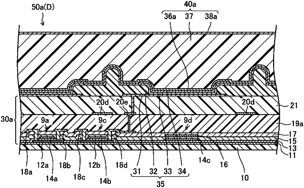
1. A display device comprising:
a base substrate;
a TFT layer which is provided on the base substrate and in which a first metal film, a first inorganic insulating film, a second metal film, a second inorganic insulating film, a third metal film, a first flattening film, a fourth metal film, and a second flattening film are sequentially layered;
a light-emitting element included in a display region and provided on the TFT layer; and
a frame region provided on a periphery of the display region;
the light-emitting element including a plurality of first electrodes provided on the second flattening film, a plurality of light-emitting element layers provided on the plurality of first electrodes respectively, and a second electrode provided to be shared on the plurality of light-emitting element layers,
wherein in the frame region, a slit passing through the second flattening film is formed in the second flattening film to surround the display region,
a first conductive layer formed by the fourth metal film is provided on the first flattening film exposed from the slit, and
a TFT included in a drive circuit is provided on the base substrate side of the first conductive layer to overlap with the first conductive layer.
|