| CPC H10K 59/131 (2023.02) [H01L 23/49838 (2013.01); H05K 1/111 (2013.01)] | 16 Claims |
|
1. A display device comprising:
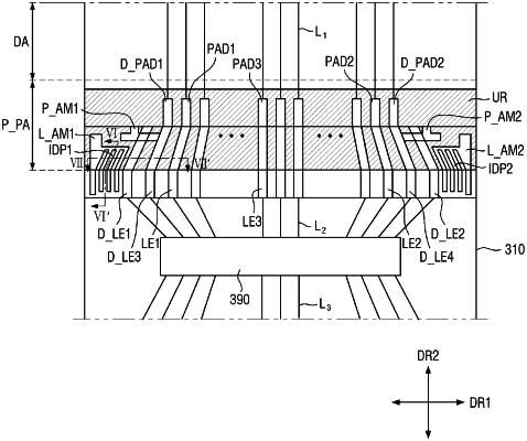
a base substrate in which a display area and a pad area disposed around the display area are defined;
a plurality of panel pads disposed on the pad area of the base substrate; and
a printed circuit board attached to the pad area of the base substrate and including:
a plurality of circuit pads including:
a first lead align mark including a plurality of first patterns passing through the first lead align mark from a surface of the first lead align mark in a thickness direction,
wherein the plurality of circuit pads further includes a first lead signal line,
wherein the plurality of panel pads includes a first panel signal line which corresponds to the first lead signal line, a first panel dummy line which is disposed between the first panel signal line and the first lead align mark, and a first panel align mark which is physically connected to the first panel dummy line,
wherein the first lead signal line and the first panel signal line are electrically connected, and
wherein the first panel align mark is separated from the first lead align mark in a plan view.
|