| CPC H10K 59/126 (2023.02) [H10K 59/1213 (2023.02); H10K 59/65 (2023.02); H10K 77/111 (2023.02); H01L 27/1222 (2013.01); H01L 29/78633 (2013.01); H01L 29/78675 (2013.01); H10K 2102/311 (2023.02)] | 20 Claims |
|
1. A display device comprising:
a display panel having a flexible characteristic; and
a rear passivation layer disposed on a rear surface of the display panel and including an opening,
wherein a pixel formed in an area of the display panel corresponding to the opening includes:
a flexible substrate including a polyimide layer, and a barrier layer disposed on the polyimide layer;
a driving transistor and a fifth transistor disposed on the substrate and including a polycrystalline semiconductor layer;
a light emitting diode receiving an output current of the driving transistor; and
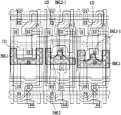
a bottom metal layer disposed between the polyimide layer and the polycrystalline semiconductor layer in a cross-sectional view and disposed around a channel of the driving transistor in a plan view.
|