| CPC H10K 59/122 (2023.02) [H10K 59/131 (2023.02); H10K 59/88 (2023.02)] | 18 Claims |
|
1. A display panel, comprising:
a display region;
a light transmitting region at a side of the display region or surrounded by the display region;
a first dummy region between the display region and the light transmitting region, the first dummy region being a non-light emitting region;
a first signal line in the display region and the first dummy region;
a display pixel unit in the display region and comprising a display pixel circuit; and
a first dummy pixel unit in the first dummy region and comprising a first dummy pixel circuit,
wherein the display pixel circuit is connected with the first signal line, and the first dummy pixel circuit is connected with the first signal line,
the display panel further comprises a second signal line and a connection element,
wherein the second signal line has a same extending direction as the first signal line, the second signal line is connected with the first signal line through the connection element, and the second signal line is connected with the first dummy pixel unit,
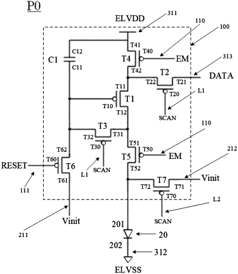
the display panel further comprises a data line, a light emitting control signal line, a first power line, a second power line, a reset control signal line, a first initialization signal line and a second initialization signal line, wherein the first dummy pixel unit further comprises a dummy element, and the first dummy pixel unit comprises a driving transistor, a data writing transistor, a threshold compensation transistor, a first light emitting control transistor, a second light emitting control transistor, a first reset transistor, a second reset transistor and a storage capacitor,
a first electrode of the storage capacitor is electrically connected with a second electrode of the threshold compensation transistor, and a second electrode of the storage capacitor is electrically connected with the first power line;
a gate electrode of the data writing transistor is electrically connected with the first signal line, and a first electrode and a second electrode of the data writing transistor are respectively electrically connected with the data line and a first electrode of the driving transistor;
a gate electrode of the threshold compensation transistor is electrically connected with the first signal line, a first electrode of the threshold compensation transistor is electrically connected with a second electrode of the driving transistor, and a second electrode of the threshold compensation transistor is electrically connected with a gate electrode of the driving transistor;
a gate electrode of the first light emitting control transistor and a gate electrode of the second light emitting control transistor are both connected with the light emitting control signal line;
a first electrode and a second electrode of the first light emitting control transistor are respectively electrically connected with the first power line and the first electrode of the driving transistor, a first electrode of the second light emitting control transistor is electrically connected with the second electrode of the driving transistor, and a second electrode of the dummy element is electrically connected with the second power line;
a gate electrode of the first reset transistor is electrically connected with the reset control signal line, a first electrode of the first reset transistor is electrically connected with the first initialization signal line, and a second electrode of the first reset transistor is electrically connected with the gate electrode of the driving transistor;
a gate electrode of the second reset transistor is electrically connected with the second signal line, and a first electrode of the second reset transistor is electrically connected with the second initialization signal line;
the dummy element is not provided with a first electrode, or in the case where the dummy element is provided with a first electrode, a second electrode of the second light emitting control transistor is not electrically connected with a first electrode of the dummy element, and a second electrode of the second reset transistor is not electrically connected with the first electrode of the dummy element.
|