| CPC H10K 59/1213 (2023.02) [G09G 3/3233 (2013.01); G09G 3/2007 (2013.01); G09G 3/3266 (2013.01); G09G 3/3275 (2013.01); G09G 2300/0426 (2013.01); G09G 2300/0809 (2013.01); G09G 2310/08 (2013.01); G09G 2320/0233 (2013.01); G09G 2320/0247 (2013.01); H01L 27/1251 (2013.01); H01L 29/78696 (2013.01)] | 4 Claims |
|
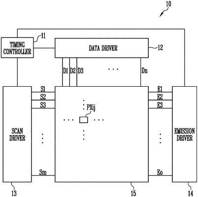
1. A display device comprising:
pixels,
wherein each of the pixels comprises:
a first transistor comprising a first gate electrode connected to a first node, a first electrode connected to a second node, and a second electrode connected to a third node;
a second transistor comprising a second gate electrode connected to a first scan line, a third electrode connected to a data line, and a fourth electrode connected to the second node;
a third transistor comprising a third gate electrode connected to the first scan line, a fifth electrode connected to the first node, and a sixth electrode connected to the third node;
a first sub-transistor comprising a fourth gate electrode connected to a second scan line, a seventh electrode connected to the first node, and a eighth electrode connected to a fifth node; and
a second sub-transistor comprising a fifth gate electrode connected to the second scan line, a ninth electrode connected to the fifth node, and a tenth electrode connected to an initialization line, and
wherein a channel width of the first sub-transistor is wider than a channel width of the second sub-transistor.
|