| CPC H10K 50/8445 (2023.02) [H10K 50/11 (2023.02); H10K 50/15 (2023.02); H10K 50/16 (2023.02); H10K 50/818 (2023.02); H10K 50/828 (2023.02); H10K 59/121 (2023.02); H10K 59/122 (2023.02); H10K 59/126 (2023.02); H10K 50/824 (2023.02); H10K 50/856 (2023.02); H10K 50/86 (2023.02); H10K 59/40 (2023.02); H10K 2102/3026 (2023.02)] | 25 Claims |
|
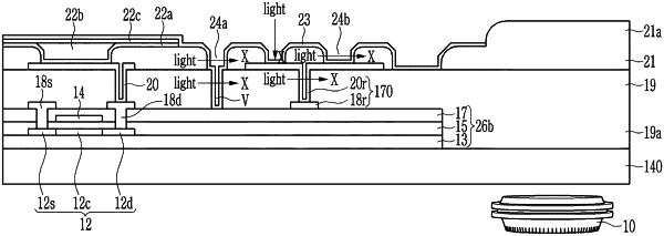
1. An electroluminescent device, comprising:
a lower substrate which is a glass substrate or an organic polymer substrate;
a lower structure disposed on the lower substrate and including an inorganic multilayer being in contact with the lower substrate; and
an upper encapsulation structure disposed on the lower structure,
wherein the lower structure includes:
a display region defined inside an outline of the inorganic multilayer in plan view; and
a light transmitting region defined inside the outline of the inorganic multilayer in plan view and having a non-through-hole structure having at least a portion surrounded by the display region in plan view,
wherein the upper encapsulation structure overlaps the light transmitting region,
wherein the display region is substantially opaque,
wherein the display region comprises a plurality of electroluminescent units, the electroluminescent unit including a reflecting electrode which is an individual layer, formed on a planarization structure and has a side portion covered by a pixel definition layer on the planarization structure, an intermediate multilayer on the reflecting electrode, and a semi-transparent electrode on the intermediate multilayer, the semi-transparent electrode being a common layer,
wherein the lower structure has an inorganic surface portion surrounding the display region and the light transmitting region in plan view, the upper encapsulation structure has an inorganic lower surface, and the inorganic lower surface of the upper encapsulation structure is in contact with the inorganic surface portion of the lower structure to form an inorganic-inorganic encapsulation contact region surrounding the display region and the light transmitting region in plan view,
wherein the electroluminescent device does not have a hole formed through both the lower substrate and the lower structure, a portion of the upper encapsulation structure, the portion corresponding to the light transmitting region, is not removed, and the portion of the upper encapsulation structure is surrounded by the inorganic-inorganic encapsulation contact region in plan view,
wherein the light transmitting region includes a plurality of display pixels,
wherein a portion of the planarization structure, the portion corresponding to the light transmitting region, is not present, and
wherein a portion of the pixel definition layer, the portion corresponding to the light transmitting region, is not present.
|