US 11,793,028 B2
Organic light emitting diode display and method for manufacturing the same
Jin-Kwang Kim, Yongin (KR); Sang-Joon Seo, Yongin (KR); Seung-Hun Kim, Yongin (KR); and Seongmin Wang, Yongin (KR)
Assigned to Samsung Display Co., Ltd., Yongin-si (KR)
Filed by Samsung Display Co., Ltd., Yongin-si (KR)
Filed on May 12, 2022, as Appl. No. 17/743,379.
Application 15/841,204 is a division of application No. 14/608,798, filed on Jan. 29, 2015, granted, now 9,853,245, issued on Dec. 26, 2017.
Application 17/743,379 is a continuation of application No. 17/080,760, filed on Oct. 26, 2020, granted, now 11,335,889.
Application 17/080,760 is a continuation of application No. 16/519,523, filed on Jul. 23, 2019, granted, now 10,854,847, issued on Dec. 1, 2020.
Application 16/519,523 is a continuation of application No. 15/841,204, filed on Dec. 13, 2017, granted, now 10,396,312, issued on Aug. 27, 2019.
Application 14/608,798 is a continuation of application No. 13/438,574, filed on Apr. 3, 2012, granted, now 8,975,660, issued on Mar. 10, 2015.
Claims priority of application No. 10-2011-0105429 (KR), filed on Oct. 14, 2011.
Prior Publication US 2022/0407034 A1, Dec. 22, 2022
Int. Cl. H01L 51/52 (2006.01); H01L 51/05 (2006.01); H10K 50/844 (2023.01); H10K 10/46 (2023.01); H01L 23/31 (2006.01); H01L 21/033 (2006.01); H01L 21/027 (2006.01); H01L 21/471 (2006.01); H01L 21/02 (2006.01); H10K 50/00 (2023.01); H10K 50/15 (2023.01); H10K 50/16 (2023.01); H10K 59/122 (2023.01)
CPC H10K 50/8445 (2023.02) [H10K 10/476 (2023.02); H01L 21/0271 (2013.01); H01L 21/02365 (2013.01); H01L 21/033 (2013.01); H01L 21/0332 (2013.01); H01L 21/471 (2013.01); H01L 23/3192 (2013.01); H10K 50/00 (2023.02); H10K 50/156 (2023.02); H10K 50/166 (2023.02); H10K 50/844 (2023.02); H10K 59/122 (2023.02)] 11 Claims
OG exemplary drawing
 
1. An organic light emitting diode (OLED) display comprising:
a substrate;
an organic light emitting diode disposed on the substrate;
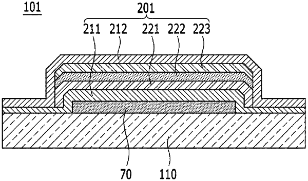
a first inorganic layer disposed on the substrate and covering the organic light emitting diode;
a second inorganic layer disposed on the first inorganic layer and contacting the first inorganic layer, the second inorganic layer entirely and directly contacting the first inorganic layer;
an organic layer disposed on the second inorganic layer and covering a relatively smaller area than the second inorganic layer; and
a third inorganic layer disposed on the organic layer, covering a relatively larger area than the organic layer, and contacting the second inorganic layer,
wherein:
the second inorganic layer covers a same area as the first inorganic layer; and
the first inorganic layer and the third inorganic layer respectively comprise silicon oxide or silicon nitride.