US 11,793,023 B2
Display apparatus having pixels around hole in substrate and touch layer overlapped with passivation layer
Jonghyun Choi, Yongin-si (KR); Kinyeng Kang, Yongin-si (KR); and Suyeon Sim, Yongin-si (KR)
Assigned to Samsung Display Co., Ltd., Yongin-si (KR)
Filed by SAMSUNG DISPLAY CO., LTD., Yongin-si (KR)
Filed on Feb. 19, 2021, as Appl. No. 17/180,622.
Application 16/273,042 is a division of application No. 15/298,082, filed on Oct. 19, 2016, granted, now 10,230,069, issued on Mar. 12, 2019.
Application 17/180,622 is a continuation of application No. 16/894,621, filed on Jun. 5, 2020, granted, now 10,978,674.
Application 16/894,621 is a continuation of application No. 16/572,462, filed on Sep. 16, 2019, granted, now 10,680,205, issued on Jun. 9, 2020.
Application 16/572,462 is a continuation of application No. 16/273,042, filed on Feb. 11, 2019, granted, now 10,431,772, issued on Oct. 1, 2019.
Claims priority of application No. 10-2016-0016360 (KR), filed on Feb. 12, 2016.
Prior Publication US 2021/0202908 A1, Jul. 1, 2021
This patent is subject to a terminal disclaimer.
Int. Cl. H10K 50/844 (2023.01); G04B 19/12 (2006.01); H10K 59/40 (2023.01); H10K 71/00 (2023.01); G04B 19/04 (2006.01); H10K 50/842 (2023.01); H10K 59/12 (2023.01); H10K 59/121 (2023.01)
CPC H10K 50/844 (2023.02) [G04B 19/04 (2013.01); G04B 19/12 (2013.01); H10K 59/40 (2023.02); H10K 71/00 (2023.02); H10K 50/8426 (2023.02); H10K 59/12 (2023.02); H10K 59/1201 (2023.02); H10K 59/121 (2023.02)] 14 Claims
OG exemplary drawing
 
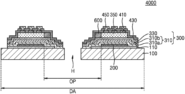
1. A display apparatus, comprising:
a substrate having a hole;
a pixel array over the substrate, the pixel array comprising a plurality of pixels that are arranged around the hole;
an encapsulation layer over the pixel array and comprising a first inorganic film, an organic film, and a second inorganic film, wherein the organic film is interposed between the first inorganic film and the second inorganic film;
a touch layer over the encapsulation layer, the touch layer comprising a touch insulating film and a plurality of touch electrodes; and
a passivation layer including organic material and located over the touch layer, wherein the passivation layer overlaps at least a part of the touch insulating film in a region between the pixel array and the hole.