| CPC H10K 50/844 (2023.02) [H10K 71/00 (2023.02); H10K 71/851 (2023.02)] | 20 Claims |

|
1. A method of fabricating a display device, the method comprising:
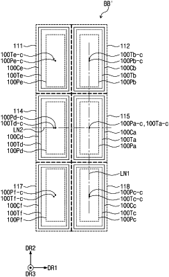
preparing a mother substrate having a first cell region and a second cell region, and a first target region and a second target region in the first cell region and the second cell region, respectively;
forming a plurality of first pixels on the first cell region;
forming a plurality of second pixels on the second cell region;
defining a first printing region in the first target region based on a location of the first target region within the mother substrate;
defining a second printing region in the second target region based on a location of the second target region within the mother substrate;
providing an encapsulation material on the first printing region overlapping the first target region to form a first encapsulation layer overlapping the plurality of first pixels;
providing the encapsulation material on the second printing region overlapping the second target region to form a second encapsulation layer overlapping the plurality of second pixels,
wherein a center of the second printing region is shifted from a center of the second target region in a specific direction; and
separating the first cell region and the second cell region from each other to form first and second display panels, respectively.
|