| CPC H10K 50/115 (2023.02) [G09G 3/3225 (2013.01); H10K 59/1213 (2023.02); G09G 2300/0842 (2013.01)] | 19 Claims |
|
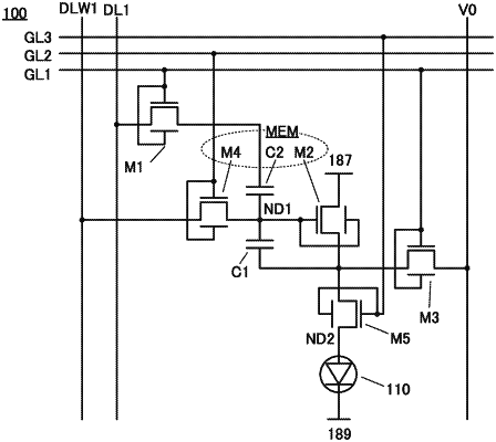
1. A display device comprising a first pixel,
wherein the first pixel includes a first light-emitting element, a color conversion layer, and a first memory circuit,
wherein the first light-emitting element exhibits blue light,
wherein the color conversion layer is configured to convert light emitted by the first light-emitting element into light having a longer wavelength,
wherein a first image signal, a first correction signal and a third correction signal are supplied to the first pixel,
wherein the first memory circuit is configured to retain the first correction signal and add the first correction signal to the first image signal, retain the third correction signal, and add the third correction signal to the first image signal, and
wherein the first pixel is configured to display an image using the first image signal, the first correction signal, and the third correction signal.
|