| CPC H10K 39/32 (2023.02) [H04N 23/84 (2023.01); H04N 25/00 (2023.01); H04N 25/79 (2023.01); H10K 30/81 (2023.02); H01L 27/14647 (2013.01); H10K 19/201 (2023.02)] | 18 Claims |
|
1. A solid-state image sensor, comprising:
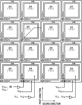
a plurality of imaging device blocks each including P×Q (where P≥2 and Q≥1) imaging devices such that P imaging devices are arranged in a first direction and Q imaging devices are arranged in a second direction different from the first direction,
wherein each imaging device includes:
a first electrode;
a charge accumulating electrode arranged with a space from the first electrode;
an isolation electrode arranged with a space from the first electrode and the charge accumulating electrode and surrounding the charge accumulating electrode;
a photoelectric conversion layer formed in contact with the first electrode and above the charge accumulating electrode with an insulating layer interposed therebetween; and
a second electrode formed on the photoelectric conversion layer,
wherein the isolation electrode includes a first isolation electrode, a second isolation electrode, and a third isolation electrode,
wherein the first isolation electrode for each imaging device included in at least a first imaging device block of the plurality of imaging device blocks is arranged adjacent to but with a space from the first electrode between imaging devices placed side by side at least along the second direction in the first imaging device block,
wherein the second isolation electrode is arranged between imaging devices in the first imaging device block,
wherein the third isolation electrode is arranged between at least the first imaging device block and a second imaging device block of the plurality of imaging device blocks, and
wherein the first isolation electrodes of the imaging devices are connected to each other.
|