| CPC H10K 30/30 (2023.02) [H10K 30/82 (2023.02); H10K 39/32 (2023.02); H10K 85/211 (2023.02); H10K 85/40 (2023.02); H10K 85/636 (2023.02); H10K 85/654 (2023.02); H10K 85/655 (2023.02); H10K 85/656 (2023.02); H10K 85/6572 (2023.02); H10K 85/6576 (2023.02)] | 31 Claims |

|
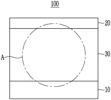
1. A photoelectric conversion device, comprising:
a first electrode and a second electrode; and
a photoelectric conversion layer between the first electrode and the second electrode,
wherein the photoelectric conversion layer includes
a first material and a second material, the first material and the second material configured to collectively define a pn junction, and
a third material different from the first material and the second material, the third material including an electron withdrawing group,
wherein the third material is an organic material including an electron donating moiety, an electron accepting moiety, and a π-conjugated linking moiety, the π-conjugated linking moiety linking the electron donating moiety with the electron accepting moiety, and
wherein the electron donating moiety includes the electron withdrawing group.
|