US 11,793,005 B2
3D semiconductor devices and structures
Deepak C. Sekar, Sunnyvale, CA (US); and Zvi Or-Bach, Haifa (IL)
Assigned to Monolithic 3D Inc., Klamath Falls, OR (US)
Filed by Monolithic 3D Inc., Klamath Falls, OR (US)
Filed on Feb. 2, 2023, as Appl. No. 18/105,041.
Application 18/105,041 is a continuation in part of application No. 17/898,475, filed on Aug. 29, 2022, granted, now 11,600,667.
Application 17/898,475 is a continuation in part of application No. 17/850,840, filed on Jun. 27, 2022, granted, now 11,462,586, issued on Oct. 4, 2022.
Application 17/850,840 is a continuation in part of application No. 17/718,932, filed on Apr. 12, 2022, granted, now 11,469,271, issued on Oct. 11, 2022.
Application 17/718,932 is a continuation in part of application No. 17/683,322, filed on Feb. 28, 2022, granted, now 11,335,731, issued on May 17, 2022.
Application 17/683,322 is a continuation in part of application No. 17/572,550, filed on Jan. 10, 2022, granted, now 11,315,980, issued on Apr. 26, 2022.
Application 17/572,550 is a continuation in part of application No. 17/542,490, filed on Dec. 5, 2021, granted, now 11,257,867, issued on Feb. 22, 2022.
Application 17/542,490 is a continuation in part of application No. 17/402,526, filed on Aug. 14, 2021, granted, now 11,227,897, issued on Jan. 18, 2022.
Application 17/402,526 is a continuation in part of application No. 17/223,822, filed on Apr. 6, 2021, granted, now 11,133,351, issued on Sep. 28, 2021.
Application 17/223,822 is a continuation in part of application No. 17/114,155, filed on Dec. 7, 2020, granted, now 11,018,191, issued on May 25, 2021.
Application 17/114,155 is a continuation in part of application No. 17/013,823, filed on Sep. 7, 2020, granted, now 10,896,931, issued on Jan. 19, 2021.
Application 17/013,823 is a continuation in part of application No. 16/409,813, filed on May 11, 2019, granted, now 10,825,864, issued on Nov. 3, 2020.
Application 16/409,813 is a continuation in part of application No. 15/803,732, filed on Nov. 3, 2017, granted, now 10,290,682, issued on May 14, 2019.
Application 15/803,732 is a continuation in part of application No. 14/555,494, filed on Nov. 26, 2014, granted, now 9,818,800, issued on Nov. 14, 2017.
Application 14/555,494 is a continuation of application No. 13/246,157, filed on Sep. 27, 2011, granted, now 8,956,959, issued on Feb. 17, 2015.
Application 13/246,157 is a continuation of application No. 13/173,999, filed on Jun. 30, 2011, granted, now 8,203,148, issued on Jun. 19, 2012.
Application 13/173,999 is a continuation of application No. 12/901,890, filed on Oct. 11, 2010, granted, now 8,026,521, issued on Sep. 27, 2011.
Prior Publication US 2023/0189537 A1, Jun. 15, 2023
This patent is subject to a terminal disclaimer.
Int. Cl. H10B 63/00 (2023.01); H01L 21/268 (2006.01); H01L 21/683 (2006.01); H01L 21/762 (2006.01); H01L 21/822 (2006.01); H01L 21/84 (2006.01); H01L 27/06 (2006.01); H01L 27/12 (2006.01); H01L 29/78 (2006.01); H01L 29/423 (2006.01); H10B 10/00 (2023.01); H10B 12/00 (2023.01); H10B 41/20 (2023.01); H10B 41/41 (2023.01); H10B 43/20 (2023.01); H10B 61/00 (2023.01); H01L 27/105 (2023.01); H10B 41/40 (2023.01); H10B 43/40 (2023.01); H10N 70/20 (2023.01); H10N 70/00 (2023.01)
CPC H10B 63/84 (2023.02) [H01L 21/268 (2013.01); H01L 21/6835 (2013.01); H01L 21/76254 (2013.01); H01L 21/8221 (2013.01); H01L 21/84 (2013.01); H01L 21/845 (2013.01); H01L 27/0688 (2013.01); H01L 27/1203 (2013.01); H01L 27/1211 (2013.01); H01L 29/42392 (2013.01); H01L 29/785 (2013.01); H01L 29/7841 (2013.01); H10B 10/00 (2023.02); H10B 12/20 (2023.02); H10B 12/50 (2023.02); H10B 41/20 (2023.02); H10B 41/41 (2023.02); H10B 43/20 (2023.02); H10B 61/22 (2023.02); H10B 63/30 (2023.02); H10B 63/845 (2023.02); H01L 27/105 (2013.01); H01L 2029/7857 (2013.01); H01L 2221/6835 (2013.01); H10B 12/056 (2023.02); H10B 12/36 (2023.02); H10B 41/40 (2023.02); H10B 43/40 (2023.02); H10N 70/20 (2023.02); H10N 70/823 (2023.02); H10N 70/8833 (2023.02)] 20 Claims
OG exemplary drawing
 
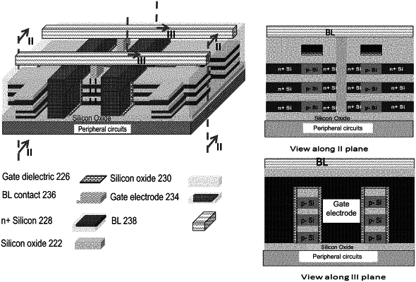
1. A semiconductor device, the device comprising:
a plurality of transistors,
wherein at least one of said plurality of transistors comprises a first single crystal source, channel, and drain,
wherein at least one of said plurality of transistors comprises a second single crystal source, channel, and drain,
wherein said second single crystal source, channel, and drain is disposed above said first single crystal source, channel, and drain,
wherein at least one of said plurality of transistors comprises a third single crystal source, channel, and drain,
wherein said third single crystal source, channel, and drain is disposed above said second single crystal source, channel, and drain,
wherein at least one of said plurality of transistors comprises a fourth single crystal source, channel, and drain, and
wherein said fourth single crystal source, channel, and drain is disposed above said third single crystal source, channel, and drain; and
a first gate structure,
wherein said first gate structure controls at least one of said first single crystal channels and at least one of said second single crystal channels.