| CPC H10B 63/34 (2023.02) [H01L 23/528 (2013.01); H10N 70/021 (2023.02); H10N 70/253 (2023.02)] | 20 Claims |
|
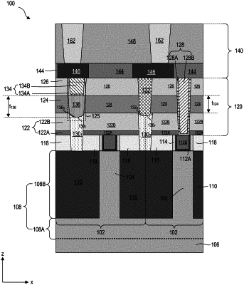
1. A semiconductor structure, comprising:
a substrate;
a gate structure over the substrate;
a source/drain (S/D) contact structure adjacent to the gate structure;
a layer of resistive material on the S/D contact structure, wherein a bottom surface of the layer of resistive material is curved or warped;
a layer of dielectric material on the layer of resistive material;
a conductor layer above the S/D contact structure, through the layer of dielectric material, and in contact with the layer of resistive material; and
an interconnect structure over and in contact with the conductor layer.
|