| CPC H10B 53/40 (2023.02) | 20 Claims |
|
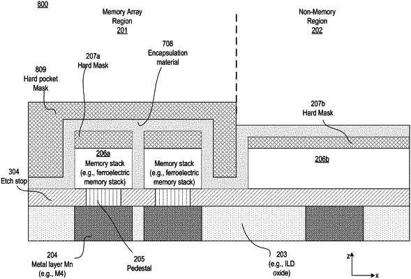
1. A method for fabricating an embedded memory, the method comprising:
applying a first pocket mask to a memory area of a die, wherein the first pocket mask is over a hard mask that extends from the memory area to a non-memory area of the die, wherein the hard mask is over a memory material stack that extends from the memory area to the non-memory area of the die, wherein the memory material stack is over at least one pedestal and an etch stop layer, and wherein the etch stop layer is non-conductive;
etching the hard mask and the memory material stack in the non-memory area down to a top surface of the etch stop layer;
depositing a protection material over the hard mask in the memory area and over the etch stop layer in the non-memory area, wherein the protection material is directly adjacent to the memory material stack; and
applying a second pocket mask to remove the protection material in the non-memory area while maintaining the protection material in the memory area.
|