| CPC H10B 51/30 (2023.02) [G11C 11/2255 (2013.01); H01L 29/40111 (2019.08); H01L 29/518 (2013.01); H01L 29/78391 (2014.09); H10B 51/20 (2023.02)] | 14 Claims |
|
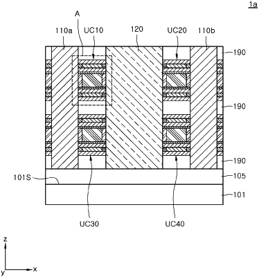
1. A semiconductor device comprising:
a substrate;
a bit line structure and a source line structure each extending in a direction perpendicular to a surface of the substrate;
a semiconductor layer disposed between the bit line structure and the source line structure on a plane parallel to the surface of the substrate;
a first ferroelectric layer disposed on a first surface of the semiconductor layer; and
a first gate electrode layer disposed on the first ferroelectric layer,
wherein the semiconductor layer, the first ferroelectric layer, and the first gate electrode layer are stacked along the direction perpendicular to the surface of the substrate.
|