| CPC H10B 43/35 (2023.02) [H01L 21/28052 (2013.01); H01L 29/4933 (2013.01); H10B 41/10 (2023.02); H10B 41/27 (2023.02); H10B 41/35 (2023.02); H10B 41/41 (2023.02); H10B 43/10 (2023.02); H10B 43/27 (2023.02); H10B 43/40 (2023.02)] | 20 Claims |
|
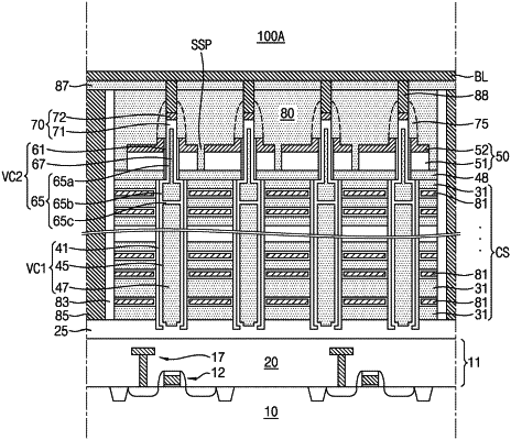
1. A three-dimensional memory device, comprising:
a source structure;
a cell stack on the source structure, the cell stack including a plurality of mold layers and a plurality of word lines alternately stacked in a vertical direction;
an upper gate electrode on the cell stack;
a string selection line separation pattern on a sidewall of the upper gate electrode;
a vertical channel structure including a lower portion and an upper portion on the lower portion;
a bit line on the vertical channel structure; and
a plug between the bit line and the vertical channel structure,
wherein the lower portion penetrates through the cell stack,
wherein the upper portion penetrates through the upper gate electrode,
wherein the vertical channel structure includes:
a lower gap-fill pattern;
an upper gap-fill pattern on the lower gap-fill pattern;
a channel layer including a lower channel layer on a sidewall of the lower gap-fill pattern, an upper channel layer on a sidewall of the upper gap-fill pattern, and an intermediate channel layer between the lower gap-fill pattern and the upper gap-fill pattern, and
wherein the lower gap-fill pattern and the upper gap-fill pattern are spaced apart from each other by the intermediate channel layer.
|