| CPC H10B 43/27 (2023.02) [H01L 29/105 (2013.01); H01L 29/1037 (2013.01)] | 18 Claims |
|
1. A method of fabricating a three-dimensional semiconductor device, comprising:
forming a first layer on a substrate;
forming a second layer on the substrate to cover the first layer;
forming a stack structure by alternately stacking a plurality of sacrificial layers and a plurality of mold insulating layers on the second layer;
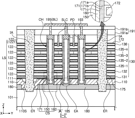
forming a channel hole penetrating through the stack structure to connect to the second layer;
extending a portion of the channel hole in a width direction, the portion of the channel hole positioned in the second layer and exposing the first layer by selectively etching the second layer through the channel hole;
forming a vertical structure by sequentially forming a vertical insulating layer and a vertical channel layer on an inner sidewall and a bottom surface of the channel hole, the vertical structure having a first extended area extending in the width direction and defined by the extended portion of the channel hole;
forming an opening penetrating through the stack structure and the second layer to connect to the first layer;
removing the first layer and a portion of the vertical insulating layer positioned in the second layer and adjacent to the first layer, through the opening, wherein a first space is formed by removing the first layer, and a second space is formed by removing the portion of the vertical insulating layer, the second space connected to the first space; and
forming a conductive layer and a conductive film, respectively, by filling in the first space and the second space with a conductive material including a first conductivity-type impurity, the conductive film connected to the conductive layer.
|