| CPC H10B 43/27 (2023.02) [H10B 43/10 (2023.02); H10B 43/35 (2023.02)] | 18 Claims |
|
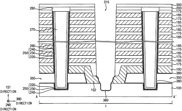
1. A method of manufacturing a vertical memory device, the method comprising:
sequentially forming a sacrificial layer structure and a support layer on a substrate;
alternately and repeatedly stacking an insulation layer and a sacrificial layer on the support layer;
forming a channel through the sacrificial layer structure, the support layer, the insulation layer, and the sacrificial layer to contact an upper surface of the substrate;
forming a first opening through the insulation layer, the sacrificial layer, and the support layer to expose at least a portion of the sacrificial layer structure;
removing the at least a portion of the sacrificial layer structure exposed by the first opening to form a first gap exposing a portion of a lower surface of the support layer;
oxidizing the exposed portion of the lower surface of the support layer, and removing the oxidized portion;
removing the sacrificial layer structure to form a second gap exposing an outer sidewall of the channel;
forming a channel connecting pattern to partially fill the second gap, the channel connecting pattern surrounding the channel and exposing a portion of the upper surface of the substrate;
oxidizing the exposed portion of the upper surface of the substrate and a sidewall of the channel connecting pattern to form an etch stop pattern;
removing the sacrificial layer to form a third gap; and
forming a gate electrode in the third gap.
|