| CPC H10B 43/27 (2023.02) [H10B 41/27 (2023.02); H10B 51/20 (2023.02); H10B 63/34 (2023.02); H10B 63/845 (2023.02)] | 13 Claims |
|
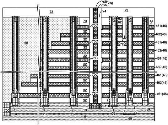
1. A memory device, comprising:
an alternating stack of insulating layers and electrically conductive layers;
a memory opening vertically extending through the alternating stack;
a memory opening fill structure located in the memory opening and comprising a vertical semiconductor channel and a vertical stack of memory elements located at levels of the electrically conductive layers;
a backside trench vertically extending through the alternating stack; and
a backside trench fill structure comprising a backside insulating material portion, wherein:
the electrically conductive layers comprise a vertically alternating sequence of first electrically conductive layers and second electrically conductive layers that are interlaced along a vertical direction;
each of the first electrically conductive layers is laterally spaced from the backside insulating material portion by a respective dielectric spacer plate; and
each of the second electrically conductive layers is in direct contact with the backside insulating material portion.
|