| CPC H10B 43/27 (2023.02) [H01L 23/5226 (2013.01); H10B 41/10 (2023.02); H10B 41/27 (2023.02); H10B 41/46 (2023.02); H10B 43/10 (2023.02); H10B 43/40 (2023.02)] | 15 Claims |
|
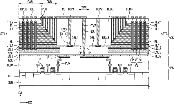
1. A semiconductor memory device, comprising:
a second substrate on a first substrate, the second substrate including a lower semiconductor layer and an upper semiconductor layer on the lower semiconductor layer;
an electrode structure including a plurality of electrodes that are stacked on the upper semiconductor layer;
a vertical channel structure that penetrates the electrode structure and is connected to the second substrate;
an interlayer dielectric layer that covers the electrode structure and directly contacts the upper semiconductor layer; and
a cutting structure that penetrates the interlayer dielectric layer and the upper semiconductor layer,
wherein the cutting structure is spaced apart from the electrode structure in a horizontal direction and at least a portion of the interlayer dielectric layer is interposed between the cutting structure and the electrode structure in the horizontal direction,
wherein the upper semiconductor layer has a first sidewall defined by the cutting structure,
wherein the lower semiconductor layer has a second sidewall adjacent to the first sidewall, and
wherein the first sidewall and the second sidewall are horizontally offset from each other.
|