| CPC H10B 20/20 (2023.02) | 20 Claims |
|
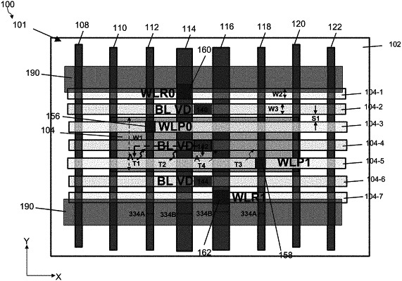
1. A semiconductor device, comprising:
a program word line and a read word line over an active region, each extending along a line direction, the program word line engaging a first transistor channel and the read word line engaging a second transistor channel;
a first metal line over and electrically connected to the program word line;
a second metal line over and electrically connected to the read word line; and
a bit line over and electrically connected to the active region,
wherein the first metal line and the second metal line are in a metal-0 (M0) interconnect layer,
wherein the program word line has a first width along a channel direction perpendicular to the line direction, the read word line has a second width along the channel direction, and
wherein the first width is less than the second width.
|