| CPC H10B 12/50 (2023.02) [H10B 12/0335 (2023.02); H10B 12/053 (2023.02); H10B 12/09 (2023.02); H10B 12/315 (2023.02); H10B 12/34 (2023.02); H10B 12/482 (2023.02); H10B 12/485 (2023.02)] | 18 Claims |
|
1. A semiconductor memory device comprising:
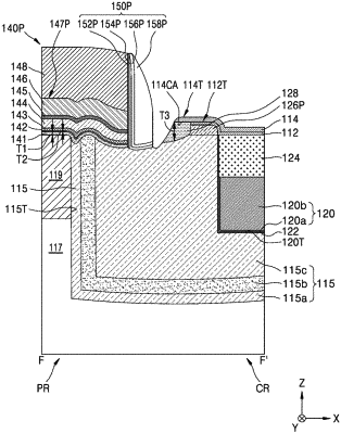
a substrate including a memory cell region, an active region in the memory cell region, a peripheral region, and a logic active region in the peripheral region;
an element isolation structure between the active region and the logic active region, the element isolation structure defining the active region and the logic active region;
an insulating layer pattern covering the active region, the insulating layer pattern including an extension portion that extends along the element isolation structure, is spaced apart from the element isolation structure, and overhangs over the element isolation structure, and the insulating layer pattern including a stacked structure in which a second insulating layer pattern having a second extension portion is on a first insulating layer pattern having a first extension portion; and
a support insulating layer filling a recess space defined between the extension portion and the element isolation structure, wherein
a portion of the element isolation structure bordering the support insulating layer has a non-flat surface, wherein
an extension length of the second extension portion is greater than an extension length of the first extension portion.
|