| CPC H05K 1/184 (2013.01) [H05K 1/0271 (2013.01); H05K 3/303 (2013.01); H05K 3/4697 (2013.01); H05K 2201/10568 (2013.01)] | 9 Claims |
|
1. A method for fabricating a carrier structure, comprising:
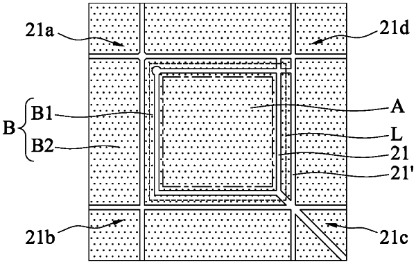
providing a substrate, wherein the substrate is defined with a chip mounting region and a surrounding region which surrounds the chip mounting region;
forming a cavity in the substrate;
forming a metal layer on the substrate to cover the cavity acting as a spacer, wherein a hollow portion is formed in the spacer, and the spacer is disposed within the surrounding region and free from communicating with the chip mounting region; and
forming a circuit layer via the metal layer,
wherein the spacer is free from being electrically connected to the circuit layer and surrounds the chip mounting region.
|