| CPC H05K 1/183 (2013.01) [H05K 1/113 (2013.01); H05K 1/185 (2013.01); H05K 2201/096 (2013.01)] | 20 Claims |
|
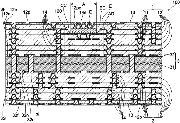
1. A component built-in wiring substrate, comprising:
a first resin insulating layer;
a first conductor layer formed on a first surface of the first resin insulating layer and including a component mounting pad;
a second conductor layer formed on a second surface of the first resin insulating layer on an opposite side with respect to the first surface of the first resin insulating layer;
a plurality of via conductors formed in the first resin insulating layer such that the plurality of via conductors is connecting the second conductor layer and the component mounting pad of the first conductor layer;
a second resin insulating layer formed on the first resin insulating layer and having a component accommodating portion penetrating through the second resin insulating layer such that the component mounting pad is positioned at bottom of the component accommodating portion; and
an electronic component positioned in the component accommodating portion of the second resin insulating layer such that the electronic component is mounted on the component mounting pad of the first conductor layer,
wherein the first conductor layer is formed such that the component mounting pad has a solid pattern formed in an entire component mounting region at the bottom of the component accommodating portion.
|