| CPC H05K 1/116 (2013.01) [H05K 1/0206 (2013.01); H05K 3/0035 (2013.01); H05K 3/0038 (2013.01); H05K 3/0047 (2013.01); H05K 3/421 (2013.01); H05K 1/184 (2013.01); H05K 3/429 (2013.01); H05K 2201/0979 (2013.01); H05K 2201/09518 (2013.01)] | 20 Claims |
|
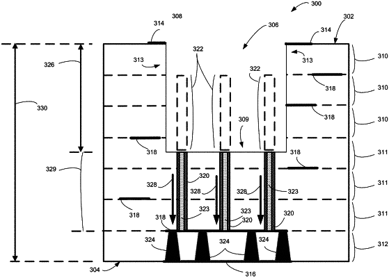
1. A printed circuit board (PCB) comprising:
at least one insulating layer comprising a first surface and a second surface opposite the first surface;
a blind slot that is plated and formed in the at least one insulating layer, the blind slot partially extending from the first surface to the second surface, wherein the blind slot includes a conductive plating bonded along a major surface of the blind slot; and
at least one via that is electrically conductive and filled, wherein the at least one via is coupled with and extends between the conductive plating of the blind slot and the second surface of the at least one insulating layer, and wherein the at least one via includes a discontinuation proximate to the major surface of the blind slot where at least a portion of the at least one via has been milled and/or drilled away.
|