| CPC H05K 1/113 (2013.01) [H05K 1/0366 (2013.01); H05K 3/4644 (2013.01); H05K 2201/0212 (2013.01); H05K 2201/068 (2013.01); H05K 2201/09136 (2013.01)] | 8 Claims |
|
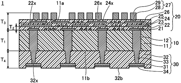
1. An interconnect substrate comprising:
a core layer including a resin layer and a through interconnect, the resin layer being mainly composed of a non-photosensitive thermosetting resin, the through interconnect extending through the resin layer, the core layer having no reinforcement member contained therein;
a first interconnect structure including a plurality of first interconnect layers and a plurality of first insulating layers mainly composed of a photosensitive resin, the first interconnect structure being laminated on a first side of the core layer; and
a second interconnect structure including a plurality of second interconnect layers and a single second insulating layer mainly composed of a photosensitive resin, the second interconnect structure being laminated on a second side of the core layer,
wherein the first interconnect layers are electrically connected to the second interconnect layers via the through interconnect,
wherein the core layer has greater rigidity than the first interconnect structure and the second interconnect structure, and
wherein a thickness of the second interconnect structure is greater than a thickness of each of the first insulating layers.
|