| CPC H05K 1/0289 (2013.01) [H01L 21/02288 (2013.01); H01L 24/26 (2013.01); H05K 1/028 (2013.01)] | 16 Claims |
|
1. A printed circuit board (PCB) comprising:
a substrate;
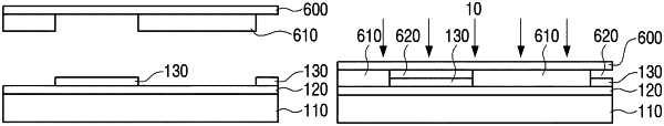
an electrode layer formed on the substrate;
a photo solder resist (PSR) layer formed on a first area of an upper part of the electrode layer, the PSR layer having a first patterned structure; and
a conductive layer formed on the PSR layer, the conductive layer having a second patterned structure that is the same as the first patterned structure, the conductive layer being configured to conduct heat and static electricity,
wherein the electrode layer comprises a second area on which the PSR layer is not formed, and
wherein the electrode layer is directly connected with a plurality of elements through the second area, without being connected with the conductive layer.
|