| CPC H05K 1/0266 (2013.01) [H01L 23/12 (2013.01); H01L 23/49811 (2013.01); H05K 1/05 (2013.01); H05K 1/184 (2013.01); H05K 3/3452 (2013.01); H05K 3/42 (2013.01)] | 7 Claims |
|
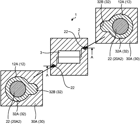
1. A circuit board comprising an interconnect and an insulating layer that covers the interconnect,
wherein the interconnect includes a first interconnect that is formed to serve as a recognition mark of which planar shape is a predetermined shape,
the insulating layer has a through-hole of which planar shape is variant and that penetrates the insulating layer in a thickness direction of the insulating layer such that an entire upper surface of the first interconnect is exposed, and
the through-hole includes
a first through-hole of which planar shape is a predetermined shape and that penetrates the insulating layer in the thickness direction such that the entire upper surface of the first interconnect is exposed; and
a second through-hole that serves as part of an inner wall surface of the first through-hole and that penetrates the insulating layer in the thickness direction.
|