| CPC H05K 1/0224 (2013.01) [H05K 1/116 (2013.01); H05K 3/107 (2013.01); H05K 2201/09036 (2013.01); H05K 2201/09636 (2013.01)] | 18 Claims |
|
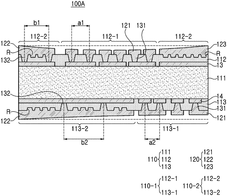
1. A printed circuit board, comprising:
an insulating layer;
a plurality of recess portions disposed on one surface of the insulating layer; and
a circuit layer disposed on the one surface of the insulating layer and including a signal pattern and a ground pattern,
wherein at least a portion of the ground pattern covers at least a portion of at least two of the plurality of recess portions, and
a depth of the plurality of recess portions is less than a thickness of the insulating layer.
|