| CPC H04N 25/79 (2023.01) [H01L 27/14647 (2013.01); H04N 25/74 (2023.01); H04N 25/771 (2023.01); H04N 25/772 (2023.01); H01L 27/1464 (2013.01)] | 20 Claims |
|
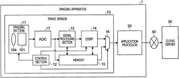
1. A stacked light receiving sensor comprising:
a first substrate that forms a first layer;
a second substrate that is joined with the first substrate and that forms a second layer;
a third substrate that is joined with the second substrate and that forms a third layer;
a pixel array section that includes a plurality of unit pixels arranged two-dimensionally in a matrix;
an analog circuit that reads a pixel signal from the pixel array section;
a logic circuit that is connected to the analog circuit and that outputs the pixel signal;
a memory that stores therein a neural network computing model;
a processing section that executes processing based on the neural network computing model, on data based on the pixel signal; and
an output section that outputs a processing result at least based on the neural network computing model to an outside, wherein
the pixel array section is disposed on the first layer,
the analog circuit is disposed on any one or more of the first to third layers, and
the logic circuit, the processing section, and the memory are disposed on any one or more of the second and third layers,
wherein a first area defined by a first perimeter of the first substrate, a second area defined by a second perimeter of the second substrate, and a third area defined by a third perimeter of the third substrate substantially overlap each other from a plan view.
|