| CPC H04N 25/766 (2023.01) [G06T 3/0018 (2013.01); G06T 3/4046 (2013.01); G06T 7/80 (2017.01); H01L 27/14616 (2013.01); H04N 25/778 (2023.01); H04N 25/779 (2023.01)] | 19 Claims |

|
1. An image sensor, comprising:
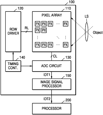
a pixel array comprising a plurality of pixels arranged in a matrix, wherein each of the pixels comprises a photoelectric conversion element configured to generate and accumulate photocharges based on an amount of external incident light, a transmission transistor configured to transmit the photocharges generated by the photoelectric conversion element to a floating diffusion node, and a reset transistor configured to reset the floating diffusion node based on a pixel power voltage, wherein the photoelectric conversion element includes a terminal to which a pixel reference voltage is applied; and
a row driver configured to control the pixels, wherein the row driver comprises a transmission control signal generator configured to provide a transmission control signal to a gate electrode of the transmission transistor,
wherein the transmission control signal generator comprises:
a first transistor of a first conductivity type and including a source electrode to which a first voltage is applied;
a second transistor of the first conductivity type and including a source electrode connected to a drain electrode of the first transistor;
a third transistor of a second conductivity type and including a source electrode to which a second voltage is applied, the second voltage being higher than the first voltage; and
a fourth transistor of the second conductivity type and including a source electrode connected to a drain electrode of the third transistor,
wherein an ON resistance of the second transistor is different from an ON resistance of the first transistor.
|