| CPC H04N 25/75 (2023.01) [H01L 27/14612 (2013.01); H01L 27/14643 (2013.01); H01L 31/02027 (2013.01); H01L 31/107 (2013.01); H04N 25/62 (2023.01); H04N 25/76 (2023.01)] | 22 Claims |
|
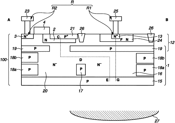
1. A photoelectric conversion device comprising:
a photoelectric conversion region including a first semiconductor region having a first conductivity type, and configured to generate a signal charge;
a second semiconductor region having a second conductivity type;
a third semiconductor region having the first conductivity type, to which the signal charge is transferred from the first semiconductor region; and
a charge accumulation region including a fourth semiconductor region having the first conductivity type, to which the signal charge is transferred from the first semiconductor region,
wherein a first potential barrier having a potential higher than a potential of the first semiconductor region between the first semiconductor region and the third semiconductor region,
wherein a second potential barrier having a potential higher than the potential of the first semiconductor region between the first semiconductor region and the fourth semiconductor region,
wherein the signal charge is transferred from the first semiconductor region to the third semiconductor region by controlling a height of the first potential barrier,
wherein, in at least a part of a period in which the signal charge is transferred from the first semiconductor region to the third semiconductor region, a reverse bias voltage for causing avalanche multiplication caused by the signal charge to occur is applied to between the second semiconductor region and the third semiconductor region, and
wherein first readout for reading out a signal that is based on the signal charge via the third semiconductor region and second readout for reading out the signal that is based on the signal charge via the fourth semiconductor region are able to be performed.
|